| CPC H01L 23/3192 (2013.01) [H01L 21/561 (2013.01); H01L 21/563 (2013.01); H01L 23/481 (2013.01); H01L 24/16 (2013.01); H01L 24/32 (2013.01); H01L 24/73 (2013.01); H01L 24/81 (2013.01); H01L 24/83 (2013.01); H01L 24/96 (2013.01); H01L 25/0652 (2013.01); H01L 25/50 (2013.01); H01L 2224/16227 (2013.01); H01L 2224/32225 (2013.01); H01L 2224/73204 (2013.01); H01L 2924/181 (2013.01)] | 20 Claims |
|
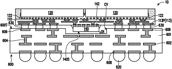
1. A semiconductor package comprising:
a circuit substrate having a first surface, a second surface opposite to the first surface and a cavity concave from the first surface, wherein the circuit substrate includes a dielectric material and a metal floor plate embedded in the dielectric material and located below the cavity, wherein the metal floor plate includes a plurality of metal plates, a location of the metal floor plate corresponds to a location of the cavity, both top and bottom surfaces of the metal floor plate are fully covered by the dielectric material, and the metal floor plate is electrically floating and isolated by the dielectric material;
a semiconductor die, disposed in the cavity and electrically connected with the circuit substrate; and
a filling material, disposed between the semiconductor die and the circuit substrate, wherein the filling material fills the cavity and encapsulates the semiconductor die to attach the semiconductor die and the circuit substrate.
|