| CPC H01L 23/31 (2013.01) [H01L 23/481 (2013.01); H01L 23/4824 (2013.01); H01L 23/5383 (2013.01); H01L 23/5384 (2013.01); H01L 23/5389 (2013.01); H01L 24/20 (2013.01); H01L 25/043 (2013.01); H01L 25/0652 (2013.01); H01L 25/0655 (2013.01); H01L 23/145 (2013.01); H01L 23/147 (2013.01); H01L 23/3128 (2013.01); H01L 23/3135 (2013.01); H01L 25/18 (2013.01); H01L 2224/04105 (2013.01); H01L 2224/12105 (2013.01); H01L 2224/131 (2013.01); H01L 2224/16227 (2013.01); H01L 2224/16235 (2013.01); H01L 2224/2518 (2013.01); H01L 2224/32225 (2013.01); H01L 2224/73204 (2013.01); H01L 2224/92125 (2013.01); H01L 2225/06541 (2013.01); H01L 2225/1035 (2013.01); H01L 2225/1041 (2013.01); H01L 2225/1058 (2013.01); H01L 2924/10253 (2013.01); H01L 2924/1434 (2013.01); H01L 2924/157 (2013.01); H01L 2924/15311 (2013.01)] | 20 Claims |
|
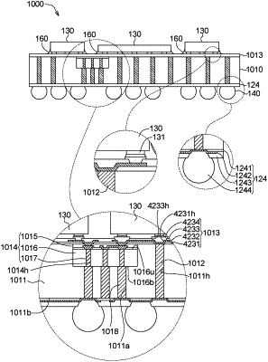
1. A semiconductor device, comprising:
a substrate; and
a body structure disposed above the substrate and comprising:
a semiconductor die having an active surface;
a molding compound encapsulating the semiconductor die and having a lower surface, an upper surface opposite to the lower surface and a through hole extending to the upper surface from the lower surface;
a conductive component formed within the through hole;
a lower redistribution layer (RDL) formed on the lower surface of the molding compound, the conductive component being exposed from the lower surface; and
a first electronic component disposed above the upper surface of the molding compound and electrically connected to the lower RDL through the conductive component,
wherein the molding compound is not present between the active surface of the semiconductor die and the lower RDL.
|