| CPC H01L 22/20 (2013.01) [H01L 21/3065 (2013.01); H01L 21/67069 (2013.01); H01L 21/68764 (2013.01)] | 20 Claims |
|
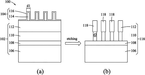
1. A method for controlling a profile of a critical dimension of a substrate, comprising:
forming a plurality of first features having a pre-process critical dimension on the substrate;
analyzing a profile of the pre-process critical dimension for the substrate; and
performing an etching process on the substrate to form a plurality of second features on the substrate, wherein the second features correspond to the first features and have a post-process critical dimension that is related to the pre-process critical dimension;
wherein the substrate is rotated during the etching process when analysis of the profile of the pre-process critical dimension reveals a first condition that the pre-process critical dimension measured at a peripheral portion of the substrate is smaller than that measured at a central portion of the substrate on average;
wherein a rotational speed at which the substrate is rotated is positively correlated to a difference between an average value of the pre-process critical dimension measured at the peripheral portion of the substrate and an average value of the pre-process critical dimension measured at the central portion of the substrate.
|