US 11,908,748 B2
Semiconductor devices and methods of forming the same
Feng-Ching Chu, Pingtung County (TW); Wei-Yang Lee, Taipei (TW); Feng-Cheng Yang, Hsinchu County (TW); and Yen-Ming Chen, Hsin-Chu County (TW)
Assigned to TAIWAN SEMICONDUCTORMANUFACTURING CO., LTD., Hsinchu (TW)
Filed by Taiwan Semiconductor Manufacturing Co., Ltd., Hsin-Chu (TW)
Filed on Nov. 15, 2022, as Appl. No. 18/055,498.
Application 18/055,498 is a continuation of application No. 17/116,808, filed on Dec. 9, 2020, granted, now 11,502,005, issued on Nov. 15, 2022.
Claims priority of provisional application 62/978,647, filed on Feb. 19, 2020.
Prior Publication US 2023/0084821 A1, Mar. 16, 2023
This patent is subject to a terminal disclaimer.
Int. Cl. H01L 21/8238 (2006.01); H01L 27/092 (2006.01); H01L 29/08 (2006.01); H01L 21/3065 (2006.01); H01L 21/308 (2006.01); H01L 29/66 (2006.01)
CPC H01L 21/823814 (2013.01) [H01L 21/308 (2013.01); H01L 21/3065 (2013.01); H01L 21/823821 (2013.01); H01L 21/823878 (2013.01); H01L 27/0924 (2013.01); H01L 29/0847 (2013.01); H01L 29/66636 (2013.01)] 20 Claims
OG exemplary drawing
 
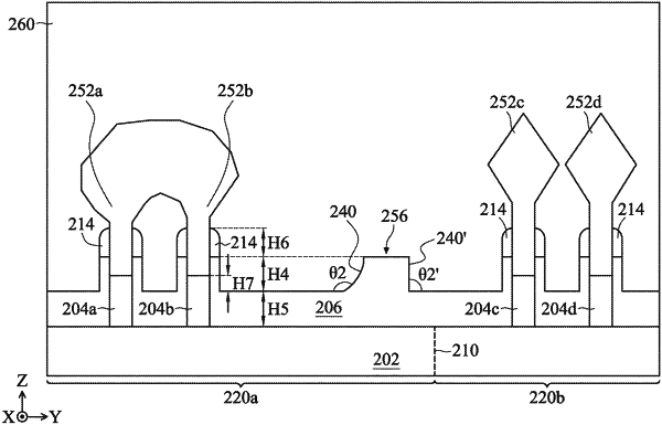
1. A semiconductor device, comprising:
a substrate having a first region and a second region of opposite conductivity types;
an isolation feature over the substrate;
a first fin protruding from the substrate and through the isolation feature in the first region;
a first epitaxial feature over the first fin;
a second fin protruding from the substrate and through the isolation feature in the second region; and
a second epitaxial feature over the second fin,
wherein a portion of the isolation feature located between the first fin and the second fin protrudes from a top surface of the isolation feature.