| CPC H01L 21/823468 (2013.01) [H01L 21/823431 (2013.01); H01L 29/0673 (2013.01); H01L 29/42392 (2013.01); H01L 29/6656 (2013.01); H01L 29/66545 (2013.01); H01L 29/66742 (2013.01); H01L 29/78618 (2013.01)] | 20 Claims |
|
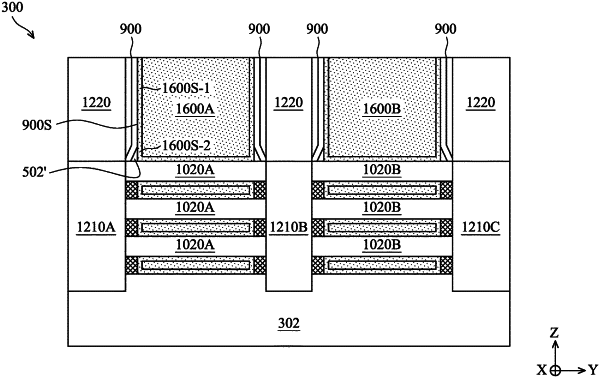
1. A semiconductor device, comprising:
a plurality of semiconductor layers vertically separated from one another;
a gate structure that comprises a lower portion and an upper portion, wherein the lower portion wraps around each of the plurality of semiconductor layers;
an etch stop layer; and
a gate spacer that extends along a sidewall of the upper portion of the gate structure and has a bottom surface;
wherein a portion of the bottom surface of the gate spacer and a top surface of a topmost one of the plurality of semiconductor layers form an angle that is less than 90 degrees; and
wherein the etch stop layer extends between the portion of the bottom surface of the gate spacer and the top surface of the topmost semiconductor layer.
|