| CPC H01L 21/823462 (2013.01) [H01L 21/823412 (2013.01); H01L 21/823431 (2013.01); H01L 21/823437 (2013.01); H01L 27/0886 (2013.01); H01L 29/42392 (2013.01); H01L 29/66545 (2013.01); H01L 29/78696 (2013.01); H01L 21/823857 (2013.01)] | 20 Claims |
|
16. A method, comprising:
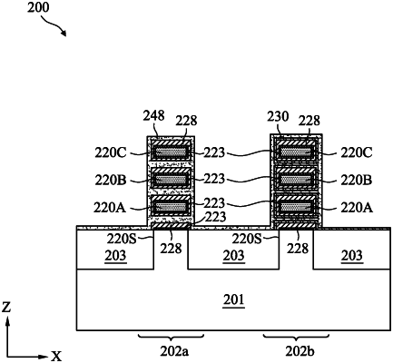
receiving a structure in a processing chamber, wherein the structure includes multiple semiconductor layers suspended over a semiconductor substrate;
forming an interfacial layer surrounding each of the semiconductor layers;
forming a gate dielectric layer over the interfacial layer and surrounding each of the semiconductor layers; and
forming a gate electrode over the gate dielectric layer and surrounding each of the semiconductor layers,
wherein the forming of the gate dielectric layer includes:
introducing a first precursor into the processing chamber for a first duration,
performing a first purging process for a second duration,
introducing a second precursor into the processing chamber for a third duration,
performing a second purging process for a fourth duration, and
repeating the introducing the first precursor, performing the first purging process, introducing the second precursor, and performing the second purging process to form the gate dielectric layer having asymmetric thicknesses around each of the semiconductor layers.
|