| CPC H01L 21/823431 (2013.01) [H01L 21/02532 (2013.01); H01L 21/32134 (2013.01); H01L 21/32139 (2013.01); H01L 21/823418 (2013.01); H01L 21/823437 (2013.01); H01L 27/0886 (2013.01); H01L 29/0847 (2013.01); H01L 29/401 (2013.01); H01L 29/41791 (2013.01); H01L 29/6653 (2013.01); H01L 29/6656 (2013.01); H01L 29/66545 (2013.01); H01L 29/66636 (2013.01); H01L 29/7848 (2013.01); H01L 21/02164 (2013.01); H01L 21/31116 (2013.01)] | 20 Claims |
|
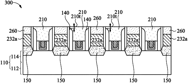
1. A semiconductor device structure, comprising:
a substrate;
a first fin structure protruding from the substrate;
an isolation layer formed around the first fin structure and covering a sidewall of the first fin structure;
a gate stack formed over the first fin structure and the isolation layer;
a first source/drain structure formed over the first fin structure and spaced apart from the gate stack;
a contact structure formed over the first source/drain structure;
a dielectric structure formed through the contact structure; and
a cap layer formed over the contact structure,
wherein the contact structure and the dielectric structure has a first slope interface that slopes downwardly from a top surface of the contact structure to a top surface of the isolation layer, and the contact structure covers the top surface of the isolation layer, and wherein the cap layer and the dielectric structure has a second slope interface that slopes downwardly from a top surface of cap layer to the top surface of the contact structure.
|