| CPC H01L 21/76897 (2013.01) [H01L 21/76816 (2013.01); H01L 21/823431 (2013.01); H01L 21/823821 (2013.01); H01L 23/5226 (2013.01); H01L 23/53261 (2013.01); H01L 27/0886 (2013.01); H01L 27/0924 (2013.01); H01L 29/41791 (2013.01); H01L 29/66795 (2013.01); H01L 29/785 (2013.01); H01L 29/66545 (2013.01); H01L 29/7848 (2013.01)] | 20 Claims |
|
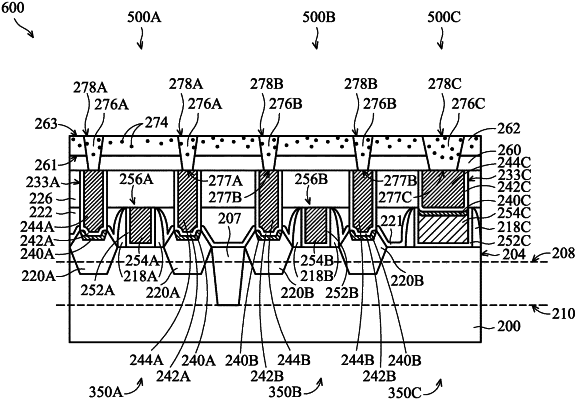
1. A semiconductor structure, comprising:
a gate structure over a substrate;
source/drain structures on opposite sides of the gate structure;
a dielectric layer over the gate structure and the source/drain structures; and
a via plug passing through the dielectric layer and comprising a first group IV element,
wherein the dielectric layer comprises a second group IV element, a first compound, and a second compound, and wherein the second compound comprises elements in the first compound and the first group IV element.
|