| CPC H01L 21/76846 (2013.01) [H01L 21/76873 (2013.01); H01L 21/76886 (2013.01); H01L 23/5226 (2013.01); H01L 23/53209 (2013.01); H01L 23/53266 (2013.01); H01L 21/76813 (2013.01); H01L 21/76831 (2013.01); H01L 21/76834 (2013.01); H01L 21/76877 (2013.01); H01L 21/76882 (2013.01); H01L 23/485 (2013.01); H01L 23/532 (2013.01); H01L 23/53295 (2013.01)] | 20 Claims |
|
1. A device comprising:
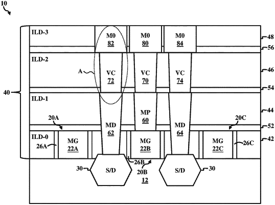
a gate structure disposed over a substrate, wherein the gate structure is disposed between a first source/drain feature and a second source/drain feature;
a cobalt-containing contact disposed directly on the first source/drain feature, wherein the cobalt-containing contact includes a cobalt-containing bulk layer, the cobalt-containing contact has an upper portion above a top surface of the gate structure, the cobalt-containing contact has a lower portion below the top surface of the gate structure, and the upper portion is disposed in a first interlayer dielectric layer and a first contact etch stop layer;
a tungsten-containing via disposed directly on the cobalt-containing contact, wherein the tungsten-containing via is disposed in a second interlayer dielectric layer and a second contact etch stop layer, wherein the tungsten-containing via includes:
a tungsten-containing bulk layer disposed on the cobalt-containing contact, and
a titanium-and-nitrogen-containing barrier layer disposed along a bottom and a sidewall of the tungsten-containing bulk layer; and
a copper-containing trace disposed directly on the tungsten-containing via, wherein the copper-containing trace is disposed in a third interlayer dielectric layer and a third contact etch stop layer.
|