| CPC H01L 21/681 (2013.01) [H01L 21/6835 (2013.01); H01L 2221/6834 (2013.01); H01L 2221/68381 (2013.01)] | 24 Claims |
|
1. A method for handling a wafer, comprising:
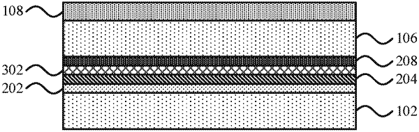
positioning a handler, which is attached to a wafer by a bonding layer that comprises a debonding layer, an optical enhancement layer, an optical boundary layer, and an anti-reflection layer; and
debonding the handler from the wafer using a laser that emits laser energy at a wavelength that is absorbed by the debonding layer, that is confined to the debonding layer by the optical enhancement layer, and that is reflected back to the debonding layer by the optical boundary layer, such that the material of the debonding layer ablates when exposed to the laser energy to release the wafer.
|