| CPC H01L 21/3115 (2013.01) [H01L 21/02192 (2013.01); H01L 21/477 (2013.01); H01L 21/823431 (2013.01); H01L 21/823857 (2013.01); H01L 27/0924 (2013.01); H01L 29/517 (2013.01); H01L 29/66795 (2013.01); H01L 29/7851 (2013.01)] | 20 Claims |
|
1. A method, comprising:
forming a fin structure on a substrate;
forming a gate opening on the fin structure;
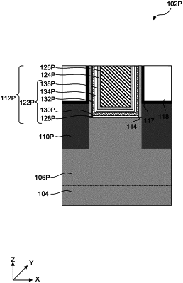
forming a metallic oxide layer within the gate opening;
forming a first dielectric layer on the metallic oxide layer, wherein the forming the first dielectric layer comprises depositing an oxide material with an oxygen areal density less than an oxygen areal density of the metallic oxide layer;
forming a second dielectric layer on the first dielectric layer;
forming a work function metal (WFM) layer on the second dielectric layer; and
forming a gate metal fill layer on the WFM layer.
|