US 11,908,700 B2
Method for manufacturing semiconductor structure
Nai-Han Cheng, Hsinchu County (TW); and Chi-Ming Yang, Hsinchu (TW)
Assigned to TAIWAN SEMICONDUCTOR MANUFACTURING COMPANY LTD., Hsinchu (TW)
Filed by TAIWAN SEMICONDUCTOR MANUFACTURING COMPANY LTD., Hsinchu (TW)
Filed on Jul. 29, 2022, as Appl. No. 17/816,374.
Application 15/892,906 is a division of application No. 14/052,973, filed on Oct. 14, 2013, granted, now 9,892,931, issued on Feb. 13, 2018.
Application 17/816,374 is a continuation of application No. 17/008,162, filed on Aug. 31, 2020, granted, now 11,482,422.
Application 17/008,162 is a continuation of application No. 15/892,906, filed on Feb. 9, 2018, granted, now 10,763,117, issued on Sep. 1, 2020.
Prior Publication US 2022/0367197 A1, Nov. 17, 2022
This patent is subject to a terminal disclaimer.
Int. Cl. H01L 21/3065 (2006.01); H01J 37/305 (2006.01); H01J 37/317 (2006.01); H01J 37/32 (2006.01)
CPC H01L 21/3065 (2013.01) [H01J 37/3053 (2013.01); H01J 37/3056 (2013.01); H01J 37/317 (2013.01); H01J 37/3172 (2013.01); H01J 37/32412 (2013.01)] 20 Claims
OG exemplary drawing
 
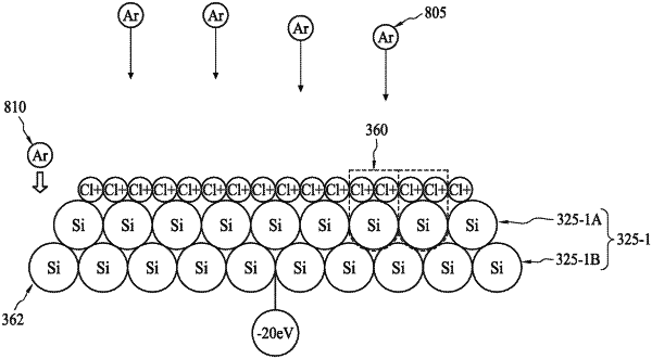
1. A method for manufacturing a semiconductor structure, comprising:
providing a substrate comprising a first atom and a second atom;
dispatching an etchant from an ionizer;
forming a compound over the substrate by bonding the first atom with the etchant;
releasing a particle from an implanter; and
removing the compound by bombarding the compound with the particle having an energy smaller than a bonding energy between the first atom and the second atom, wherein the etchant and the particle comprise different ions.