| CPC H01L 21/28141 (2013.01) [H01L 21/0234 (2013.01); H01L 21/28518 (2013.01); H01L 21/31055 (2013.01); H01L 21/31116 (2013.01); H01L 21/823456 (2013.01); H01L 21/823468 (2013.01); H01L 29/0847 (2013.01); H01L 29/4236 (2013.01); H01L 29/42372 (2013.01); H01L 29/45 (2013.01); H01L 29/4983 (2013.01); H01L 29/6653 (2013.01); H01L 29/6656 (2013.01); H01L 29/66545 (2013.01); H01L 29/66795 (2013.01); H01L 29/785 (2013.01); H01L 29/7851 (2013.01); H01L 29/7856 (2013.01)] | 20 Claims |
|
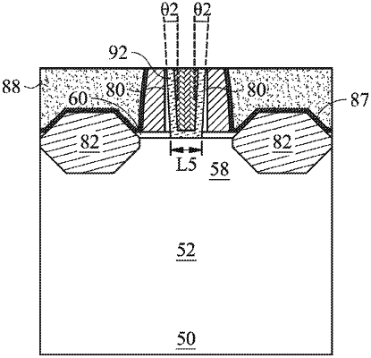
1. A device, comprising:
a plurality of source/drain regions formed in a substrate;
a gate structure over the substrate between the plurality of source/drain regions, wherein the gate structure comprises one or more gate dielectric layers and one or more gate electrode layers; and
a plurality of spacers surrounding the gate structure, wherein a first spacer of the plurality of spacers contacts the one or more gate dielectric layers, wherein the first spacer has a first thickness at a first location and a second thickness at a second location, wherein the first location is farthest from the substrate and the second location is between the first location and the substrate, and wherein a first sidewall of the first spacer that contacts the one or more gate dielectric layers extends at an angle between the first location and the second location, the angle is with respect to a direction that is perpendicular to a major surface of the substrate, and the angle is greater than or equal to 3 degrees.
|