| CPC H01L 21/0274 (2013.01) [H01L 21/56 (2013.01); H01L 21/6835 (2013.01); H01L 21/78 (2013.01); H01L 23/3128 (2013.01); H01L 23/49827 (2013.01); H01L 23/49838 (2013.01); H01L 23/544 (2013.01); H01L 24/05 (2013.01); H01L 24/08 (2013.01); H01L 24/19 (2013.01); H01L 24/20 (2013.01); H01L 21/568 (2013.01); H01L 22/14 (2013.01); H01L 24/13 (2013.01); H01L 24/14 (2013.01); H01L 25/0657 (2013.01); H01L 25/105 (2013.01); H01L 2221/68318 (2013.01); H01L 2221/68359 (2013.01); H01L 2221/68372 (2013.01); H01L 2221/68381 (2013.01); H01L 2223/5442 (2013.01); H01L 2223/54426 (2013.01); H01L 2223/54486 (2013.01); H01L 2224/02311 (2013.01); H01L 2224/02317 (2013.01); H01L 2224/02319 (2013.01); H01L 2224/02331 (2013.01); H01L 2224/02379 (2013.01); H01L 2224/04105 (2013.01); H01L 2224/05548 (2013.01); H01L 2224/08265 (2013.01); H01L 2224/12105 (2013.01); H01L 2224/13024 (2013.01); H01L 2224/1403 (2013.01); H01L 2224/14181 (2013.01); H01L 2224/32145 (2013.01); H01L 2224/32225 (2013.01); H01L 2224/48091 (2013.01); H01L 2224/48227 (2013.01); H01L 2224/73265 (2013.01); H01L 2224/73267 (2013.01); H01L 2224/92244 (2013.01); H01L 2224/94 (2013.01); H01L 2225/0651 (2013.01); H01L 2225/06568 (2013.01); H01L 2225/1023 (2013.01); H01L 2225/1058 (2013.01); H01L 2924/15311 (2013.01); H01L 2924/37001 (2013.01)] | 20 Claims |
|
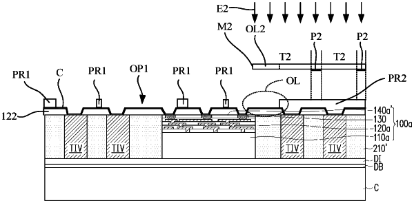
1. A method, comprising:
performing a first exposure process using a first mask to transfer a first layout pattern of the first mask onto a photoresist layer;
performing a first development process to form a first wiring opening with the first layout pattern in the photoresist layer;
after performing the first development process, performing a second exposure process using a second mask to transfer a second layout pattern of the second mask onto the photoresist layer, wherein the second layout pattern transferred onto the photoresist layer is substantially aligned with and overlaps an overlay region of the first wiring opening;
performing a second development process to form a second wiring opening with the second layout pattern in the photoresist layer, wherein the first wiring opening and the second wiring opening are communicated at the overlay region; and
after performing the second development process, forming a conductive wiring in the first wiring opening and the second wiring opening.
|