| CPC H01L 21/02389 (2013.01) [H01L 21/0254 (2013.01); H01L 21/02458 (2013.01); H01L 21/3212 (2013.01); H01L 29/8122 (2013.01)] | 18 Claims |
|
1. A method of manufacturing a vertical device, comprising:
providing a GaN-based semiconductor substrate, wherein the semiconductor substrate has a front surface and a rear surface opposite to the front surface, and the semiconductor substrate is etched from the front surface to form a trench;
sequentially forming a P-type semiconductor layer and an N-type semiconductor layer on a bottom wall and side walls of the trench and the front surface of the semiconductor substrate, wherein the trench is partially filled with the P-type semiconductor layer, wherein doping ions in the P-type semiconductor layer and the N-type semiconductor layer are implemented by in-situ doping;
planarizing the N-type semiconductor layer and the P-type semiconductor layer, and retaining the P-type semiconductor layer and the N-type semiconductor layer in the trench; and
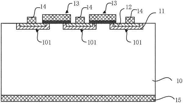
respectively forming a gate structure, a source electrode, and a drain electrode, wherein the gate structure is located at a gate area of the front surface of the semiconductor substrate, the source electrode is located on two sides of the gate structure, and the drain electrode is located on the rear surface of the semiconductor substrate.
|