| CPC H01L 21/0217 (2013.01) [G02F 1/1368 (2013.01); H01L 21/0228 (2013.01); H01L 21/02211 (2013.01); H01L 29/786 (2013.01)] | 12 Claims |
|
1. A manufacturing method for forming a passivation layer of a thin film transistor, the passivation layer comprising a first silicon nitride layer, a second silicon nitride layer formed on the first silicon nitride layer, and a third silicon nitride layer formed on the second silicon nitride layer, wherein an etching rate of the first silicon nitride layer is less than etching rates of the second silicon nitride layer and the third silicon nitride layer, the manufacturing method comprising:
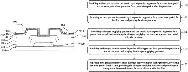
providing a silane precursor into an atomic layer deposition apparatus for a preset time period, and allowing the silane precursor to remain in the atomic deposition apparatus for a preset time period after the providing;
providing an inert gas into the atomic layer deposition apparatus for a preset time period for the first time, and purging the silane precursor;
providing a nitrogen supplying precursor into the atomic layer deposition apparatus for a preset time period, and allowing the nitrogen supplying precursor to remain in the atomic deposition apparatus for a preset time period after the providing;
providing the inert gas into the atomic layer deposition apparatus for a preset time period for the second time, and purging the nitrogen supplying precursor; and
repeating for a preset number of times the steps of providing the silane precursor, providing the inert gas for the first time, providing the nitrogen supplying precursor and providing the inert gas for the second time to form the first silicon nitride layer, the second silicon nitride layer, and the third silicon nitride layer successively, wherein the first silicon nitride layer, the second silicon nitride layer, and the third silicon nitride layer collectively constitute a silicon nitride thin film.
|