| CPC G11C 7/106 (2013.01) [G11C 7/1087 (2013.01); G11C 7/222 (2013.01); H03K 3/037 (2013.01)] | 20 Claims |
|
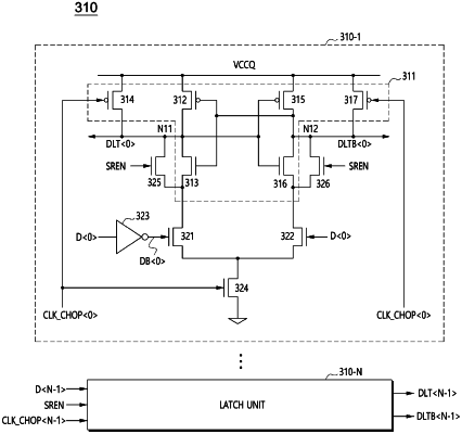
1. A latch circuit comprising:
a first detection unit configured to generate an output signal by detecting a level of an input terminal in response to a transition of a control clock signal during a normal read operation; and
a second detection unit configured to generate the output signal by detecting the level of the input terminal in response to the control clock signal during a state information read operation,
wherein the control clock signal transits repeatedly during the normal read operation, and the control clock signal is fixed to a first logic level during the state information read operation.
|