| CPC G11C 5/025 (2013.01) [G11C 7/06 (2013.01); G11C 7/1069 (2013.01); G11C 7/1096 (2013.01); G11C 8/08 (2013.01); G11C 8/10 (2013.01)] | 30 Claims |
|
1. A semiconductor device comprising:
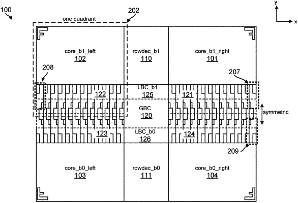
a memory circuit having a plurality of quadrants arranged at corners of the memory circuit and surrounding a bank control component;
wherein a first quadrant of the plurality of quadrants includes a first bit cell core and a first set of input output circuits, the first quadrant defined by a rectangular boundary that encloses portions of two perpendicular edges of the memory circuit;
wherein a second quadrant of the plurality of quadrants includes a second bit cell core and a second set of input output circuits, wherein there is a first axis between the first quadrant and the second quadrant about which the first set of input output circuits and the second set of input output circuits are symmetrical; and
wherein a third quadrant of the plurality of quadrants includes a third bit cell core and a third set of input output circuits, the third quadrant being symmetrical with the first quadrant along a second axis that is perpendicular to a direction of wordlines in the first bit cell core.
|