| CPC G11C 13/0038 (2013.01) [G11C 13/004 (2013.01); G11C 13/0026 (2013.01); G11C 13/0028 (2013.01); G11C 2213/79 (2013.01)] | 16 Claims |
|
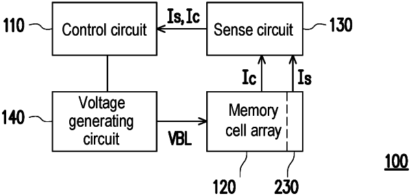
1. A resistive memory apparatus, comprising:
a memory cell array, comprising a plurality of memory cells, each of the memory cells comprising a resistive switching element;
at least one dummy transistor, electrically isolated from the resistive switching element; and
a control circuit, coupled to the memory cell array and the at least one dummy transistor, and configured to provide a first bit line voltage, a source line voltage and a word line voltage to the at least one dummy transistor so that the at least one dummy transistor outputs a saturation current and determine a value of a second bit line voltage for driving the memory cells according to the saturation current,
wherein the control circuit is configured to determine which one of a plurality of saturation current intervals the saturation current of the at least one dummy transistor is in, and drive the memory cells according to the second bit line voltage corresponding to the saturation current interval.
|