| CPC G09G 3/3266 (2013.01) [G09G 3/20 (2013.01); G09G 3/3677 (2013.01); G11C 19/28 (2013.01); G09G 2300/0426 (2013.01); G09G 2310/0267 (2013.01); G09G 2310/0286 (2013.01); G09G 2310/08 (2013.01); G09G 2320/0223 (2013.01)] | 6 Claims |
|
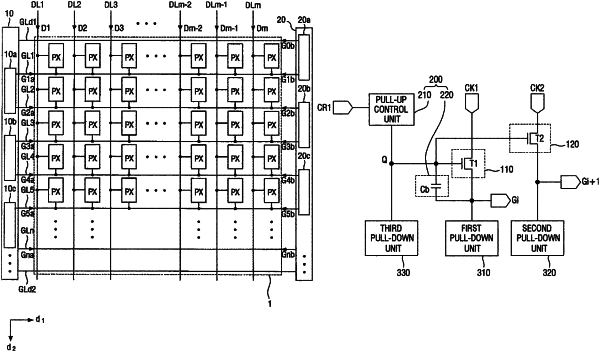
1. A display device comprising:
a display panel comprising a plurality of pixels connected to a first gate line, a second gate line, and a third gate line that are adjacent to one another;
a first gate driving circuit on a first side of the plurality of pixels and comprising a first stage for outputting first and second gate signals having phases that are different from each other; and
a second gate driving circuit on a second side of the plurality of pixels that is opposite the first side of the plurality of pixels, and comprising a second stage for outputting third and fourth gate signals having phases that are different from each other,
wherein the first stage is configured to provide the first gate signal to a first side of the second gate line,
wherein the second stage is configured to provide the fourth gate signal to a second side of the second gate line,
wherein the first stage is configured to provide the second gate signal to a first side of the third gate line,
wherein the second stage is configured to provide the third gate signal to a second side of the first gate line, and
wherein the first stage comprises:
a first pull-up portion for outputting a first clock signal as the first gate signal in accordance with a signal provided to a control node; and
a second pull-up portion for outputting a second clock signal having a phase that is different from a phase of the first clock signal as the second gate signal in accordance with the signal provided to the control node.
|