| CPC G09G 3/3258 (2013.01) [G09G 3/3233 (2013.01); G09G 2300/0426 (2013.01); G09G 2300/0819 (2013.01); G09G 2300/0842 (2013.01); G09G 2300/0861 (2013.01); G09G 2310/0278 (2013.01); G09G 2310/061 (2013.01); G09G 2310/08 (2013.01); G09G 2320/0233 (2013.01); G09G 2320/045 (2013.01)] | 22 Claims |
|
1. A display apparatus, comprising: light emitting elements arranged in a matrix; pixel circuits arranged in a matrix; a scan signal line; a data signal line; an initial signal line; a light emitting control line; a first power supply line; a first reset line; a second reset line; and a third reset line, wherein:
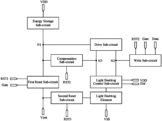
the pixel circuits correspond to the light emitting elements in a one to one way, each of the pixel circuits is configured to drive a corresponding light emitting element to emit light, and the pixel circuit comprises a first reset sub-circuit, a node control sub-circuit, a light emitting control sub-circuit, and a second reset sub-circuit;
the first reset sub-circuit is connected with the first reset line, the scan signal line, the initial signal line and a first node, respectively, and configured to provide a signal of the initial signal line for the first node under control of the first reset line and the scan signal line;
the node control sub-circuit is connected with the scan signal line, the second reset line, the data signal line, the first node, a second node, a third node and a first power supply line, respectively, and configured to provide a signal of the data signal line for the second node under control of the scan signal line and the second reset line, compensate for the first node through the second node and the third node until a voltage of the first node satisfies a threshold condition, and provide a signal of the second node for the third node under control of the first node;
the light emitting control sub-circuit is connected with the light emitting control line, the first power supply line, the second node, the third node and the light emitting element, respectively, and configured to provide a signal of the first power supply line for the second node and a signal of the third node for the light emitting element under control of the light emitting control line;
the second reset sub-circuit is connected with the third reset line, the initial signal line and the light emitting element, respectively, and configured to provide a signal of the initial signal line for the light emitting element under control of the third reset line; and
the third reset line connected with pixel circuits located in an ith row is electrically connected with the first reset line connected with pixel circuits located in an (i+1)th row, wherein 1≤i<M, and M is a total number of rows of the pixel circuits, and wherein:
each pixel circuit comprises: a storage capacitor, the storage capacitor comprises a first plate and a second plate, the first plate is connected with the first power supply line, and the second plate is connected with the first node;
an orthographic projection of the first plate on a base partially overlaps an orthographic projection of the second plate on the base, the first plate is provided with a via, and the via of the first plate exposes the second plate;
the scan signal line, the first reset line and the second reset line are located on a side of the second plate, and the light emitting control line is located on a side of the second plate away from the first reset line; and
the first reset line is located on a side of the scan signal line away from the second plate, and the second reset line is located on a side of the scan signal line close to the second plate.
|