| CPC G09G 3/2092 (2013.01) [G09G 2300/0842 (2013.01); G09G 2320/0233 (2013.01); G09G 2320/0276 (2013.01)] | 20 Claims |
|
1. A display device comprising:
a display panel comprising:
a group of pixels, wherein each of the group of pixels comprise one or more pixels that each control a luminance of a color component of a corresponding pixel; and
display driving circuitry configured to program, onto the group of pixels, image data to be displayed via the group of pixels;
a processor; and
a memory accessible by the processor;
wherein the processor is configured to:
receive image data configured to be displayed via the group of pixels, wherein the image data comprises gray level data for a first pixel of the group of pixels;
convert the gray level data to first voltage data;
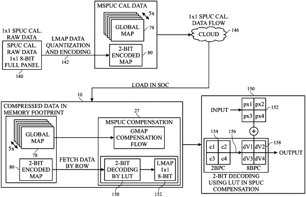
fetch second voltage data from encoding data of a compensation map, the second voltage data comprising 1×1 pixel uniformity compensation data for at least a portion of the group of pixels including the first pixel, wherein the 1×1 pixel uniformity compensation data comprises compensation data to mitigate non-uniformity between at least a portion of the group of pixels when supplied with a same electrical input signal and wherein the second voltage data is configured to be inputted to a look-up table configured to decode the second voltage data into voltage compensation data for the first pixel, and wherein the look-up table stores at least one voltage compensation offset value corresponding to the 1×1 pixel uniformity compensation data for the one or more pixels of the group of pixels;
determine a voltage compensation offset value associated with the first pixel based on the second voltage data;
generate compensated voltage data based in part on the voltage compensation offset value and the first voltage data;
convert the compensated voltage data to compensated gray level data; and
transmit the compensated gray level data to the display driving circuitry associated with the first pixel.
|