| CPC G09G 3/20 (2013.01) [G09G 3/3275 (2013.01); G09G 3/3685 (2013.01); G09G 3/3688 (2013.01); G09G 5/008 (2013.01); G09G 2310/027 (2013.01); G09G 2310/0291 (2013.01); G09G 2310/08 (2013.01); G09G 2320/02 (2013.01); G09G 2320/0223 (2013.01); G09G 2320/0233 (2013.01); G09G 2370/08 (2013.01)] | 7 Claims |
|
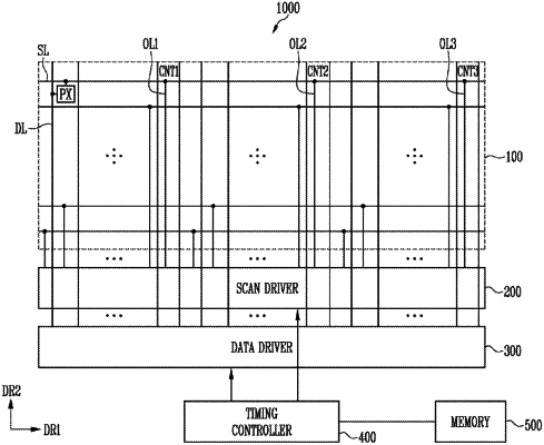
1. A display device, comprising:
a display area including pixels connected to data lines and scan lines, wherein the display area includes a plurality of signal output lines connected to each of the scan lines through a plurality of contacts;
a data driver including a first data driving circuit disposed at a side of the display area to drive the data lines;
a scan driver disposed at the side of the display area to drive the scan lines; and
a timing controller for controlling the data driver and the scan driver,
wherein the display area includes first to third pixel blocks continuous in a first direction, and
each of the first to third pixel blocks includes first to k-th (where k is an integer greater than 2) data lines included in a driving region,
wherein the first data driving circuit comprises:
output buffers which respectively output data signals to the first to k-tin data lines of the data lines; and
an output delay controller which transmits the data signals to the output buffers through first to k-th transmission lines, and controls delay times of the data signals output to the first to k-th transmission lines based on position information of a pixel row to which the data signals are to be supplied and a positional relationship between the contacts and the first to K-th data lines,
wherein the delay times increase in the first direction away from the the driving region or increase in a direction opposite the first direction away from the contacts in the driving region,
wherein times at which the data signals are output from the output buffers to the first to k-th data lines are respectively adjusted based on the delay times,
wherein the plurality of signal output lines comprises:
first output lines connected to each of the scan lines in the first pixel block;
second output lines connected to each of the scan lines in the second pixel block; and
third output lines connected to each of the scan lines in the third pixel block,
wherein the scan lines extend in the first direction, and the first to third output lines extend in a second direction crossing the first direction,
wherein the first output lines connect a first scan line of the scan lines in a first contact among the contacts,
wherein the second output lines connect the first scan line in a second contact among the contacts,
wherein the third output lines connect the first scan line in a third contact among the contacts,
wherein the delay times decrease from the first pixel block to the third pixel block,
wherein a portion of the first scan line between the first contact and the second contact has a largest resistance component, and
wherein a portion of the first scan line on a right side of the third contact has a smallest resistance component.
|