| CPC G06V 40/1318 (2022.01) [G02F 1/13338 (2013.01); G06F 3/0412 (2013.01)] | 19 Claims |
|
1. A display panel, comprising:
a display substrate, the display substrate including a plurality of pixel units;
a touch layer and a fingerprint recognition layer disposed on the display substrate,
wherein the touch layer includes one or more touch units,
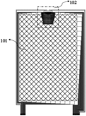
the fingerprint recognition layer includes one or more primary fingerprint recognition units, and each of the primary fingerprint recognition units includes NSFPS sub-fingerprint recognition units corresponding to Npixel ones of the pixel units, where NSFPS and Npixel are positive integers;
a thin film encapsulation layer disposed on the display substrate;
a first insulating layer disposed on the thin film encapsulation layer;
a first metal layer disposed on the first insulating layer;
a second insulating layer disposed on the first metal layer and provided with at least one via hole;
a second metal layer disposed on the second insulating layer and connected with the first metal layer by the via hole; and
a third insulating layer disposed on the second metal layer.
|