US 11,907,636 B2
Integrated circuit layout generation method
Ke-Ying Su, Hsinchu (TW); Jon-Hsu Ho, Hsinchu (TW); Ke-Wei Su, Hsinchu (TW); Liang-Yi Chen, Hsinchu (TW); Wen-Hsing Hsieh, Hsinchu (TW); Wen-Koi Lai, Hsinchu (TW); Keng-Hua Kuo, Hsinchu (TW); Kuopei Lu, Hsinchu (TW); Lester Chang, Hsinchu (TW); and Ze-Ming Wu, Hsinchu (TW)
Assigned to TAIWAN SEMICONDUCTOR MANUFACTURING COMPANY, LTD., Hsinchu (TW)
Filed by TAIWAN SEMICONDUCTOR MANUFACTURING COMPANY, LTD., Hsinchu (TW)
Filed on Jul. 8, 2022, as Appl. No. 17/860,919.
Application 17/860,919 is a division of application No. 16/950,999, filed on Nov. 18, 2020, granted, now 11,392,749.
Application 16/950,999 is a continuation of application No. 16/389,679, filed on Apr. 19, 2019, granted, now 10,846,456, issued on Nov. 24, 2020.
Claims priority of provisional application 62/665,660, filed on May 2, 2018.
Prior Publication US 2022/0343054 A1, Oct. 27, 2022
Int. Cl. G06F 30/398 (2020.01); G03F 1/70 (2012.01); G03F 1/36 (2012.01); G06F 30/20 (2020.01)
CPC G06F 30/398 (2020.01) [G03F 1/36 (2013.01); G03F 1/70 (2013.01); G06F 30/20 (2020.01)] 20 Claims
OG exemplary drawing
 
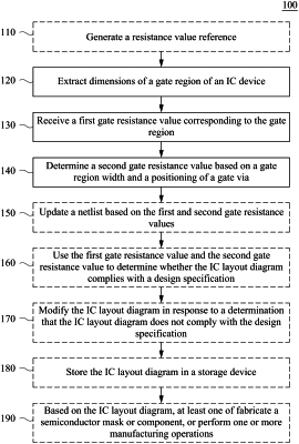
1. A method of generating an integrated circuit (IC) layout diagram, the method comprising:
receiving a first gate resistance value of a gate region in an IC layout diagram, the first gate resistance value corresponding to a location of a gate via positioned within an active region and along a width of the gate region extending across the active region;
determining a second gate resistance value based on the location and the width;
using the first and second resistance values by performing an alternating current (AC) simulation based on the IC layout diagram to determine that the IC layout diagram does not comply with a design specification; and
based on the non-compliance with the design specification, modifying the IC layout diagram.