| CPC G06F 3/0659 (2013.01) [G06F 3/0619 (2013.01); G06F 3/0653 (2013.01); G06F 3/0673 (2013.01); G11C 29/42 (2013.01); G11C 29/44 (2013.01)] | 17 Claims |
|
1. A memory sub-system comprising:
a memory device;
a processing device coupled to the memory device and configured to control cache memory for the memory device to store data prior to storing the data on the memory device; and
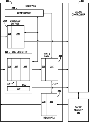
an interface of the memory sub-system comprising error correction circuitry and a comparator, wherein the interface is coupled to the processing device and configured to:
receive a write command addressed to a first address and a read command addressed to a second address from a host;
receive data corresponding to the write command from the host;
store the write command and the read command in a command buffer of the interface;
store the data in a write buffer of the interface;
determine, using the comparator of the interface, whether the first address matches the second address while the write command and the read command are stored in the command buffer;
determine, using the comparator of the interface, whether the write command was inserted into the command buffer prior to insertion of the read command into the command buffer by comparing a first identifier (ID) of the write command and a second ID of the read command, wherein the first ID and the second ID are assigned sequentially based on an order in which commands are received from the host; and
responsive to determining that the first address matches the second address and that the write command was inserted into the command buffer prior to inserting the read command into the command buffer:
drop the read command and the second address from the command buffer by sending a signal from the comparator to the error correction circuitry to cause the error correction circuitry to mark the read command as being erroneous without regard to performing an error check on the read command and without regard to whether the read command passes an error check if performed, wherein a memory sub-system controller is configured to delete the read command responsive to the read command being marked by the error correction circuitry;
forward the data from the write buffer directly to a read buffer of the interface via lines that couple the write buffer to the read buffer; and
provide the data to the host from the read buffer; and
responsive to determining that the first address does not match the second address, provide the read command and the second address to the processing device.
|