| CPC G06F 3/0619 (2013.01) [G06F 3/0617 (2013.01); G06F 3/0656 (2013.01); G06F 3/0658 (2013.01); G06F 3/0679 (2013.01)] | 20 Claims |
|
1. A non-volatile memory device, comprising:
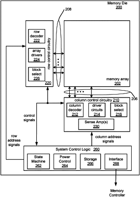
a control circuit configured to connect to a plurality of columns, each column comprising one or more bit lines each connected to a corresponding plurality of memory cells, the plurality of columns including a plurality of regular columns and one or more spare columns, the control circuit comprising:
a plurality of sense amplifiers each configured to read data from the memory cells connected to a corresponding one or more bit lines of the plurality of columns;
a plurality of sets of internal data latches, each set of internal data latches configured to store data associated with a corresponding one of the sense amplifiers; and
an input-output interface, including a plurality of data buffers, configured to provide data to an external data bus,
the control circuit configured to:
perform a read operation by each of the sense amplifiers on a plurality of memory cells;
store results of the read operation by each of the sense amplifiers in the corresponding set of internal data latches;
compress the results of the read operation by each of the sense amplifiers within the corresponding set of internal data latches;
transfer the compressed results of the read operation to the input-output interface;
re-order bits of the compressed results of the read operation;
subsequent to re-ordering the compressed results of the read operation, replace the compressed results of the read operation from defective ones of the regular columns with corresponding compressed results of the read operation from spare columns within the input-output interface by multiplexing the re-ordered bits of the compressed results of the read operation;
store the re-ordered bits of the compressed results with the compressed results of the read operation from defective ones of the regular columns replaced with corresponding compressed results of the read operation from spare columns in the plurality of data buffers; and
transfer the compressed results of the read operation, including replaced compressed results of the read operation, from the plurality of data buffers to the external data bus.
|