| CPC G06F 3/0604 (2013.01) [G06F 3/064 (2013.01); G06F 3/0607 (2013.01); G06F 3/0632 (2013.01); G06F 3/0658 (2013.01); G06F 3/0659 (2013.01); G06F 3/0673 (2013.01); G06F 3/0679 (2013.01); G06F 9/30101 (2013.01); G06F 9/30123 (2013.01); G06F 9/3897 (2013.01); G06F 9/4881 (2013.01); G06F 9/5016 (2013.01); G06F 12/0607 (2013.01); G06F 12/084 (2013.01); G06F 12/0811 (2013.01); G06F 12/0815 (2013.01); G06F 12/0828 (2013.01); G06F 12/0831 (2013.01); G06F 12/0855 (2013.01); G06F 12/0857 (2013.01); G06F 12/0875 (2013.01); G06F 12/0891 (2013.01); G06F 12/10 (2013.01); G06F 12/1009 (2013.01); G06F 13/124 (2013.01); G06F 13/1642 (2013.01); G06F 13/1663 (2013.01); G06F 13/1668 (2013.01); G06F 13/4027 (2013.01); H03M 13/015 (2013.01); H03M 13/098 (2013.01); H03M 13/1575 (2013.01); H03M 13/276 (2013.01); H03M 13/2785 (2013.01); G06F 12/0833 (2013.01); G06F 12/0846 (2013.01); G06F 12/0851 (2013.01); G06F 12/0862 (2013.01); G06F 2212/1008 (2013.01); G06F 2212/1016 (2013.01); G06F 2212/1024 (2013.01); G06F 2212/1048 (2013.01); G06F 2212/304 (2013.01); G06F 2212/452 (2013.01); G06F 2212/6024 (2013.01); G06F 2212/657 (2013.01)] | 20 Claims |
|
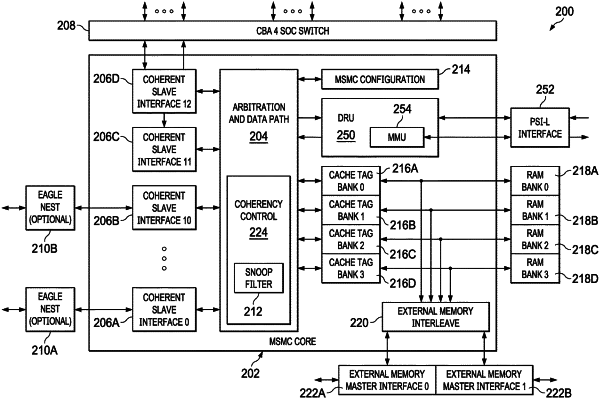
1. A processing system comprising:
a plurality of processors including a first processor;
a cache memory coupled to the plurality of processors; and
a shared memory controller comprising:
circuitry configured to receive a memory management command having a specification to perform a memory management operation to load data into a memory location of the cache memory before the first processor executes an input/output instruction that requests the data from the memory location;
formatting circuitry configured to format the memory management command into a formatted command; and
routing circuitry configured to route the formatted command based on the specification; and
response circuitry configured to receive a response indicating the data was loaded into the memory location.
|