| CPC G06F 3/0446 (2019.05) [G06F 3/0412 (2013.01); G06F 2203/04111 (2013.01)] | 23 Claims |
|
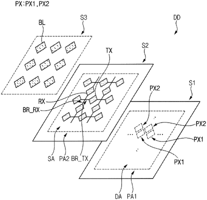
1. A display device comprising:
a pixel layer including a plurality of first pixel units, each including a plurality of first sub-light emitting regions, and a plurality of second pixel units, each including a plurality of second sub-light emitting regions;
a touch sensing layer including a plurality of sensing electrodes disposed on the pixel layer, and a plurality of driving electrodes electrically insulated from the sensing electrodes and disposed on the pixel layer, at least some of the sensing electrodes and the driving electrodes each includes a dummy pattern defining a plurality of dummy openings overlapping the first sub-light emitting regions when viewed in a plan view, and a sensing pattern electrically insulated from the dummy pattern and spaced apart from the first sub-light emitting regions and the second sub-light emitting regions when viewed in a plan view; and
a light blocking pattern disposed on the touch sensing layer, defining a plurality of light blocking openings overlapping the first sub-light emitting regions when viewed in a plan view, and overlapping the first pixel units when viewed in a plan view.
|