| CPC G06F 3/0412 (2013.01) [G06F 3/0446 (2019.05); H10K 59/40 (2023.02); G06F 2203/04112 (2013.01); H10K 59/12 (2023.02); H10K 77/10 (2023.02)] | 17 Claims |
|
1. An electronic device comprising:
an electronic module; and
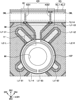
a sensing unit detecting an external input, the sensing unit being divided into a hole area overlapping the electronic module, an active area surrounding the hole area, and a peripheral area adjacent to the active area and including a first sensing electrode and a second sensing electrode disposed in the active area and spaced apart from each other,
wherein:
the first sensing electrode comprises first main patterns, first neighboring patterns having a shape different from a shape of the first main patterns, and a hole pattern connected to the adjacent first neighboring patterns;
the second sensing electrode comprises second main patterns, second neighboring patterns adjacent the hole area and having a shape different from a shape of the second main patterns, second connection patterns connected to the second main patterns, and a routing pattern connected to the adjacent second neighboring patterns; and
the hole pattern is disposed in the hole area, and the routing pattern is disposed in the peripheral area.
|