| CPC G06F 12/1009 (2013.01) [G06F 3/064 (2013.01); G06F 3/0616 (2013.01); G06F 3/0688 (2013.01); G06F 12/0246 (2013.01); G06F 12/109 (2013.01); G06F 3/0659 (2013.01); G06F 3/0662 (2013.01); G06F 2212/1016 (2013.01); G06F 2212/7201 (2013.01); G06F 2212/7202 (2013.01); G06F 2212/7205 (2013.01)] | 18 Claims |
|
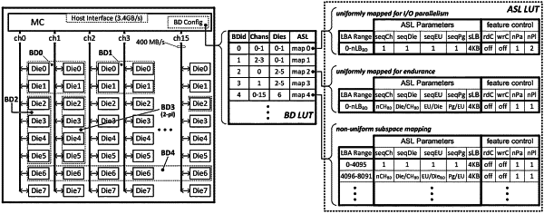
1. A memory controller to control nonvolatile memory, the memory controller comprising:
circuitry to map host-provided addresses to physical addresses in the nonvolatile memory according to one of two alternate mappings; and
a register to store a programmably-defined address mapping parameter;
wherein the circuitry is to map data, received with sequentially-received write requests, to a number of respective storage units of a type of storage unit, wherein the type is a same one from a group of channels, dies, erase units, planes, and pages, wherein the number of the respective storage units of the type is variable dependent on a value of the programmably-defined address mapping parameter;
wherein each host-provided address comprises a first portion and a second portion, and
for a first one of the two alternate mappings, the first portion of each host-provided address is mapped to a first number of first storage units of the nonvolatile memory and the second portion of each host-provided address is mapped to a first number of second storage units of the nonvolatile memory,
for a second one of the two alternate mappings, the first portion of each host-provided address is mapped by said circuitry to a second number of the first storage units and the second portion of each host-provided address is mapped by said circuitry to a second number of the second storage units;
the first storage units are respective units of a first type of units from the group, and the second storage units are respective units of a second type of units from the group, and
one of the first portion and the second portion can be mapped to a non-power of two set of structural addresses and the circuitry to map is to perform modulo arithmetic on each host-provided address to recover the other of the first portion and the second portion, with no address in a range of addresses represented by the first portion and the second portion remaining unmapped to a storage location in the nonvolatile memory; and
circuitry to service the write requests by issuing commands accompanied by the physical addresses, the physical addresses being generated using the one of the two alternate mappings.
|