US 11,906,898 B2
Method of manufacturing phase shift photo masks
Chun-Chieh Tien, Kaohsiung (TW); Cheng-Hsuen Chiang, Miaoli (TW); Chih-Ming Chen, Dasi Township (TW); Cheng-Ming Lin, Siluo Township (TW); Yen-Wei Huang, Tainan (TW); Hao-Ming Chang, Pingtung (TW); Kuo-Chin Lin, Tainan (TW); and Kuan-Shien Lee, Taichung (TW)
Assigned to TAIWAN SEMICONDUCTOR MANUFACTURING COMPANY, LTD., Hsinchu (TW)
Filed by TAIWAN SEMICONDUCTOR MANUFACTURING CO., LTD., Hsinchu (TW)
Filed on Aug. 10, 2020, as Appl. No. 16/989,744.
Application 16/989,744 is a continuation of application No. 15/905,543, filed on Feb. 26, 2018, granted, now 10,739,671, issued on Aug. 11, 2020.
Claims priority of provisional application 62/584,556, filed on Nov. 10, 2017.
Prior Publication US 2020/0371425 A1, Nov. 26, 2020
Int. Cl. G03F 1/32 (2012.01); G03F 1/38 (2012.01); H01L 21/308 (2006.01); G03F 1/80 (2012.01)
CPC G03F 1/32 (2013.01) [G03F 1/38 (2013.01); G03F 1/80 (2013.01); H01L 21/3083 (2013.01)] 20 Claims
OG exemplary drawing
 
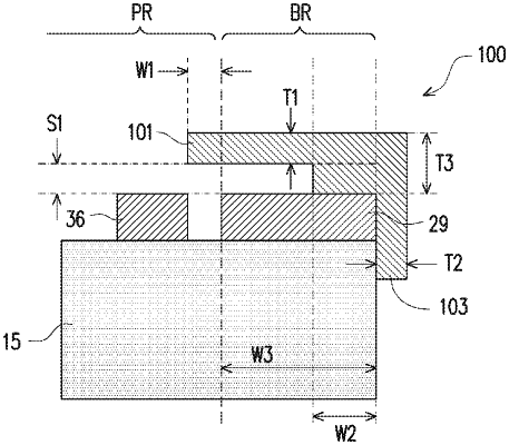
1. An apparatus for a photo mask manufacturing operation comprising an etching hard cover, wherein:
the etching hard cover is a reusable ceramic comprising a sintered body,
the etching hard cover has a rectangular frame shape having a rectangular opening and a rectangular frame portion defining the rectangular opening,
the frame portion includes a main cover portion that covers a border region of the photo mask to be manufactured, and
a bottom surface of the main cover portion includes an abutting portion to abut the photo mask, when the etching hard cover is placed on the photo mask, the border region of the photo mask is covered by the etching hard cover such that the etching hard cover is in contact with a light blocking layer disposed at the border region.