| CPC G02F 1/1345 (2013.01) [G02F 1/13452 (2013.01); G02F 1/136204 (2013.01); G02F 1/136254 (2021.01); G02F 1/136286 (2013.01); H01L 27/0288 (2013.01); H10K 59/131 (2023.02)] | 16 Claims |
|
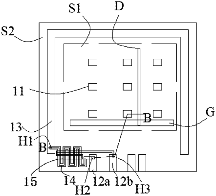
1. A display substrate, comprising:
a base substrate;
a transistor, an anti-static wire, a first anti-static resistor, and a first ground bonding pad on the base substrate; and
an anti-static electrode and a common electrode bonding pad which is configured to receive a common voltage,
wherein a first terminal of the first anti-static resistor is electrically connected to a first end of the anti-static wire, and a second terminal of the first anti-static resistor is electrically connected to the first ground bonding pad,
the first anti-static resistor is at a different layer from a layer at which the anti-static wire is located and a layer at which the first ground bonding pad is located,
an orthographic projection of the anti-static electrode on the base substrate overlaps an orthographic projection of the first anti-static resistor on the base substrate, the anti-static electrode and the first anti-static resistor are insulated and spaced apart from each other in a thickness direction of the display substrate, and the anti-static electrode and the common electrode bonding pad receive a same voltage signal.
|