| CPC G02F 1/133614 (2021.01) [G02F 1/133603 (2013.01); G02F 1/133605 (2013.01); G02F 1/133608 (2013.01); G02F 1/133612 (2021.01); G02F 1/133621 (2013.01); G02F 2201/346 (2013.01); G02F 2202/36 (2013.01)] | 18 Claims |
|
1. A display device comprising:
a liquid crystal panel; and
a light source plate disposed behind the liquid crystal panel configured to provide the liquid crystal panel with light,
wherein the light source plate includes:
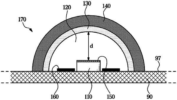
a printed circuit board (PCB) having a mounting surface;
a light emitting diode (LED) chip mounted on the mounting surface;
a transparent resin disposed on the LED chip to substantially surround the LED chip;
a light conversion layer configured to convert a wavelength of light emitted from the LED chip, the light conversion layer substantially surrounding an outer surface of the transparent resin;
a barrier layer covering the light conversion layer from an outside; and
an auxiliary light conversion layer disposed on the mounting surface adjacent to the LED chip, wherein a portion of the auxiliary light conversion layer above the mounting surface is substantially surrounded by the transparent resin and the auxiliary light conversion layer is configured to convert a wavelength of light emitted from the LED chip.
|