US 11,906,830 B2
Display device
Seong Min Wang, Seongnam-si (KR); Beohm Rock Choi, Seoul (KR); and Yong Ho Yang, Suwon-si (KR)
Assigned to Samsung Display Co., Ltd., Yongin-si (KR)
Filed by Samsung Display Co., Ltd., Yongin-si (KR)
Filed on Nov. 4, 2022, as Appl. No. 17/980,579.
Application 17/980,579 is a continuation of application No. 17/167,004, filed on Feb. 3, 2021, granted, now 11,493,795.
Application 17/167,004 is a continuation of application No. 16/203,614, filed on Nov. 29, 2018, granted, now 10,942,385, issued on Mar. 9, 2021.
Claims priority of application No. 10-2018-0037659 (KR), filed on Mar. 30, 2018.
Prior Publication US 2023/0056635 A1, Feb. 23, 2023
This patent is subject to a terminal disclaimer.
Int. Cl. G09G 5/00 (2006.01); G02F 1/1333 (2006.01); H10K 50/86 (2023.01); H10K 50/842 (2023.01); H10K 59/60 (2023.01); G06V 40/13 (2022.01); G06V 40/12 (2022.01)
CPC G02F 1/1333 (2013.01) [G02F 1/13338 (2013.01); G06V 40/13 (2022.01); H10K 50/8426 (2023.02); H10K 50/865 (2023.02); H10K 59/60 (2023.02); G02F 2201/086 (2013.01); G02F 2201/58 (2013.01); G02F 2202/28 (2013.01); G06V 40/12 (2022.01); G06V 40/1306 (2022.01); G06V 40/1318 (2022.01)] 22 Claims
OG exemplary drawing
 
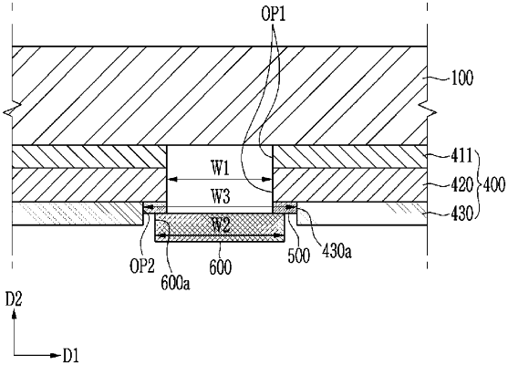
1. A display device comprising:
a display panel having a first side including a display area configured to emit light and a second side opposite to the first side;
a sensor having a first surface facing the display panel;
a first adhesive layer disposed between the first surface of the sensor and the display panel; and
a second adhesive layer disposed on a side surface of the sensor,
wherein the second adhesive layer and the first adhesive layer contact each other.