| CPC G02F 1/025 (2013.01) [G02F 2202/104 (2013.01); G02F 2202/105 (2013.01)] | 8 Claims |
|
1. A method, comprising:
patterning a base component to impart:
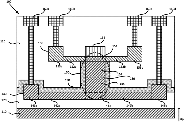
a lower waveguide that is separated from a substrate of the base component by a first layer of an insulator, the lower waveguide comprising:
a lower hub, made of monocrystalline silicon;
a lower ridge, made of monocrystalline silicon that extends in a first direction from the lower hub;
a first lower wing, made of monocrystalline silicon, that extends in a third direction, perpendicular to the first direction, from the lower hub;
a second lower wing, made of monocrystalline silicon, that extends in a fourth direction, opposite from the third direction, from the lower hub;
a first lower interface, made of monocrystalline silicon, located on a distal end of the first lower wing relative to the lower hub and extending upward in the first direction from the first lower wing; and
a second lower interface, made of monocrystalline silicon, located on a distal end of the second lower wing relative to the lower hub and extending in the first direction from the second lower wing;
an upper ridge for an upper waveguide that is located above the lower waveguide and is separated from the lower waveguide by a predefined height;
depositing a gate oxide layer on the lower waveguide;
depositing a second layer of the insulator on the gate oxide layer;
etching the second layer of the insulator to define a cavity of a predefined shape; and
forming polycrystalline silicon wings for the upper waveguide in the cavity.
|