| CPC G02B 6/136 (2013.01) [G02B 6/125 (2013.01)] | 8 Claims |
|
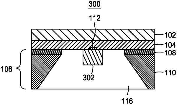
1. An apparatus, comprising:
a photonic wafer comprising an electrical layer and a layer disposed on a substrate, wherein the layer comprises at least one optical waveguide that is disposed between the electrical layer and the substrate; and
an end-face coupler, wherein a portion of the end-face coupler is within a portion of the substrate underneath the at least one optical waveguide, and wherein the end-face coupler is configured to direct an optical signal to or from the optical waveguide and comprises an optical interface for end-face coupling.
|