| CPC G02B 5/208 (2013.01) [G02B 1/002 (2013.01); H01L 27/14625 (2013.01)] | 21 Claims |
|
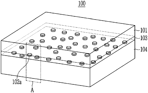
1. An optical filter, comprising:
a near-infrared absorbing layer including a first material, the first material being configured to absorb light in a first wavelength spectrum within a near-infrared wavelength spectrum,
a compensation layer adjacent to the near-infrared absorbing layer, the compensation layer including a second material different from the first material, and
a metamaterial structure spaced apart from the near-infrared absorbing layer via the compensation layer, the metamaterial structure being configured to absorb, reflect, and/or scatter light in a second wavelength spectrum at least partially overlapped with the first wavelength spectrum such that the second wavelength spectrum at least partially overlaps the near-infrared wavelength spectrum.
|