| CPC G02B 1/115 (2013.01) [C03C 17/3435 (2013.01); C03C 2217/734 (2013.01); C03C 2217/78 (2013.01); C03C 2218/155 (2013.01)] | 22 Claims |
|
1. An article comprising:
an inorganic oxide substrate comprising opposing major surfaces; and
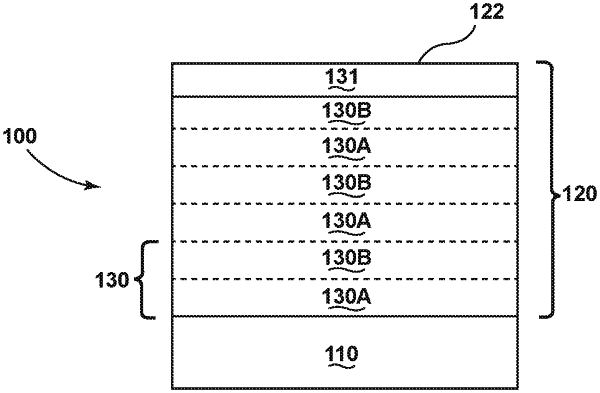
an optical film structure disposed on a first major surface of the inorganic oxide substrate, the optical film structure comprising a physical thickness from about 50 nm to less than 500 nm, a plurality of alternating high index and low index layers with a first low index layer on the first major surface, and a capping low index layer,
wherein each low index layer comprises a silicon-containing oxide and each high index layer comprises silicon nitride or silicon oxynitride,
wherein the article exhibits a hardness of 8 GPa or greater measured at an indentation depth of about 100 nm or a maximum hardness of 9 GPa or greater measured over an indentation depth range from about 100 nm to about 300 nm, the hardness and the maximum hardness measured by a Berkovich Indenter Hardness Test,
wherein the first low index layer is in direct contact with the first major surface of the substrate,
wherein a high index layer is adjacent to the capping low index layer and it has an optical thickness from about 45 nm to about 450 nm, and
further wherein one of the high refractive index layers in the optical film structure is the thickest layer in the layers of the optical film structure below the capping index layer.
|