| CPC G01R 31/275 (2013.01) [G01R 1/0466 (2013.01); G01R 1/0491 (2013.01)] | 20 Claims |
|
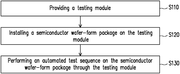
1. A testing module for a semiconductor wafer-form package, comprising:
a circuit board structure;
first connectors, disposed over the circuit board structure and connected to the circuit board structure;
a first connecting structure, disposed over and distant from the circuit board structure;
second connectors and third connectors, disposed over and connected to the first connecting structure, wherein the third connectors are configured to transmit electric signals for testing the semiconductor wafer-form package being placed over the circuit board structure; and
a first bridge connector, electrically coupling the circuit board structure and the first connecting structure by connecting the second connectors and the first connectors,
wherein the semiconductor wafer-form package is surrounded by the circuit board structure, the first connectors, the first bridge connector, the first connecting structure, the second connectors, and the third connectors.
|