| CPC C03C 17/42 (2013.01) [C03C 17/002 (2013.01); C03C 17/02 (2013.01); C03C 17/25 (2013.01); C03C 17/30 (2013.01); C03C 2203/52 (2013.01); C03C 2204/08 (2013.01); C03C 2217/213 (2013.01); C03C 2217/285 (2013.01); C03C 2217/77 (2013.01); C03C 2217/78 (2013.01); C03C 2218/112 (2013.01); C03C 2218/32 (2013.01); G06F 3/041 (2013.01)] | 17 Claims |
|
1. A cover glass included in a rear cover for an electronic device, comprising:
a glass plate forming at least a portion of the electronic device; and
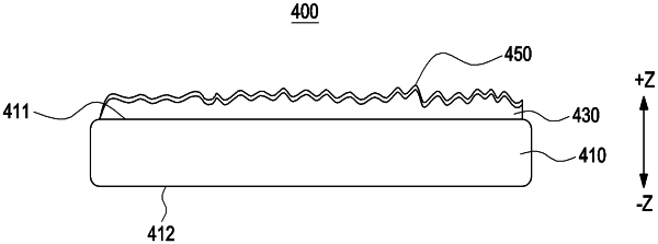
a first coat layer disposed on a surface of the glass plate, the first coat layer at least partially including a network structure with multiple protrusion-and-depression shapes formed by inorganic polysilazane coated on the surface of the glass plate, wherein the first coat layer has a hazing exceeding 5% and a transmittance of less than 91%, the first coat layer being steam hardening-processed in a temperature range of 100° C. to below 200° C. for a time range of 30 minutes to 120 minutes during a first hardening step, and processed with peroxide in a temperature range at 30° C. to 200° C. for three hours during a second hardening step after the first hardening step,
a second coat layer disposed on a surface of the first coat layer and including a shape corresponding to the network structure of the first coat layer,
wherein the first coat layer includes silicon (Si), oxygen (O), and at least one impurity,
wherein Si—O bonds are at least 80% by-weight of mass of the first coat layer, and
wherein the hazing denotes a state in a middle of changing from transparent to opaque depending on a percent of the hazing,
wherein the multiple protrusion-and-depression shapes includes a plurality of valley portions and peak portions,
wherein the plurality of valley portions have a thickness ranging from 300 nm to 600 nm, and the peak portions have a thickness ranging from 0.6 μm to 2 μm, and
wherein a thickness of the first coat layer is implemented in a range of a thickness of the plurality of valley portions and a thickness of the peak portions so that a degree of the hazing is not lowered.
|