| CPC B81C 1/00896 (2013.01) [B81C 2203/0785 (2013.01)] | 31 Claims |
|
1. A method comprising:
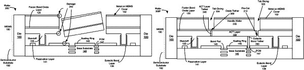
forming a pre-cut in a tab region disposed between a first die and a second die, wherein the tab region structurally connects the first die to the second die, wherein the first die comprises a first Micro-Electromechanical System (MEMS) device eutecticly bonded to a first semiconductor device, and wherein the second die comprises a second MEMS device eutecticly bonded to a second semiconductor device, wherein the tab region includes a handle wafer layer disposed over a fusion bond oxide layer that is disposed on an actuator (ACT) layer, wherein the tab region is positioned above a semiconductor tab region, and wherein the tab region, the first die, the second die, and the semiconductor tab region form a cavity therein;
tab dicing a first region of the tab region that corresponds to the pre-cut that cuts through the handle wafer layer, the fusion bond oxide layer, and the ACT layer to expose the semiconductor tab region;
tab dicing a second region of the tab region that cuts through the handle wafer layer and that leaves a portion of the ACT layer underneath to form an ACT tether, wherein the ACT tether structurally maintains the tab region in place and above the semiconductor tab region; and
subsequent to the tab dicing the first region and the second region, removing the tab region.
|