| CPC B01L 3/502792 (2013.01) [B01L 3/50273 (2013.01); B01L 2200/0673 (2013.01); B01L 2300/06 (2013.01); B01L 2300/089 (2013.01); B01L 2300/12 (2013.01); B01L 2300/165 (2013.01); B01L 2300/168 (2013.01); B01L 2400/0427 (2013.01)] | 17 Claims |
|
1. A device for fast manipulation of many thousands of microdroplets simultaneously using optically-mediated electrowetting comprising:
a first composite wall comprising:
a first substrate;
a first transparent conductor layer on the first substrate having a thickness in the range 70 to 250 nm;
a photoactive layer activated by electromagnetic radiation in the wavelength range 400-1000 nm on the first transparent conductor layer having a thickness in the range 300-1000 nm and
a first dielectric layer on the photoactive layer; and
a first anti-fouling layer on the first dielectric layer;
a second composite wall comprising:
a second substrate;
a second conductor layer on the second substrate having a thickness in the range 70 to 250 nm; and
a second dielectric layer on the second conductor layer; and
a second anti-fouling layer on the second dielectric layer
the device further comprising:
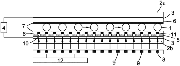
one or more spacers for holding the first and second walls apart by a pre-determined amount to define a microfluidic space adapted to contain microdroplets, wherein the spacer comprises a bead, a pillar or a ridge;
an A/C source to provide a voltage of between 10V and 50V across the first and second composite walls connecting the first and second conductor layers so as to be below the dielectric breakdown voltage of the first and second dielectric layers;
at least one source of electromagnetic radiation having an energy higher than the bandgap of a photoexcitable layer adapted to impinge on the photoactive layer to induce corresponding ephemeral electrowetting locations on the surface of the first dielectric layer; and
a microprocessor for manipulating points of impingement of the electromagnetic radiation on the photoactive layer so as to vary the disposition of the ephemeral electrowetting locations thereby creating at least one electrowetting pathway along which microdroplets may be caused to move;
wherein the device is configured to performing chemical analyses carried out on multiple analytes simultaneously.
|