| CPC A61L 2/10 (2013.01) [A61L 2/26 (2013.01); H01L 33/483 (2013.01); H01L 33/56 (2013.01); A61L 2202/122 (2013.01)] | 20 Claims |
|
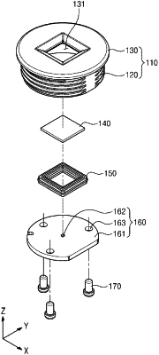
1. A sterilization device comprising:
a main body;
a circuit board disposed in the main body;
a light source disposed on the circuit board and configured to emit sterilizing light; and
a transparent unit configured to protect the light source from an outside and comprising a material that transmits the sterilizing light emitted from the light source,
wherein the light source comprises:
a mesa including a first semiconductor layer, an active layer, and a second semiconductor layer;
a first electrode electrically connected to the first semiconductor layer; and
a second electrode disposed on the second semiconductor layer and electrically connected to the second semiconductor layer,
wherein the first electrode includes a first contact region disposed on the outer area of the first semiconductor layer and a second contact region at least partially surrounded by the mesa, and
wherein a distance between the transparent unit and the circuit board is greater than a height of the light source.
|