US 12,232,425 B2
Magnetoresistive random access memory
Hui-Lin Wang, Taipei (TW); Si-Han Tsai, Taichung (TW); Dong-Ming Wu, Taichung (TW); Chen-Yi Weng, New Taipei (TW); Ching-Hua Hsu, Kaohsiung (TW); Ju-Chun Fan, Tainan (TW); Yi-Yu Lin, Taichung (TW); Che-Wei Chang, Taichung (TW); Po-Kai Hsu, Taichung (TW); and Jing-Yin Jhang, Tainan (TW)
Assigned to UNITED MICROELECTRONICS CORP., Hsin-Chu (TW)
Filed by UNITED MICROELECTRONICS CORP., Hsin-Chu (TW)
Filed on Nov. 21, 2023, as Appl. No. 18/515,273.
Application 18/515,273 is a continuation of application No. 17/348,776, filed on Jun. 16, 2021, granted, now 11,864,468.
Claims priority of application No. 202110533886.6 (CN), filed on May 17, 2021.
Prior Publication US 2024/0099154 A1, Mar. 21, 2024
This patent is subject to a terminal disclaimer.
Int. Cl. G11C 11/00 (2006.01); G11C 11/16 (2006.01); H01F 10/32 (2006.01); H10B 61/00 (2023.01); H10N 50/10 (2023.01); H10N 50/80 (2023.01); H10N 50/85 (2023.01)
CPC H10N 50/10 (2023.02) [G11C 11/161 (2013.01); H01F 10/3254 (2013.01); H10B 61/00 (2023.02); H10N 50/80 (2023.02); H10N 50/85 (2023.02)] 5 Claims
OG exemplary drawing
 
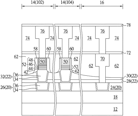
1. A magnetic random access memory (MRAM) device, comprising:
a first array region, a second array region, and a logic region on a substrate;
a first magnetic tunneling junction (MTJ) on the first array region;
a first spacer adjacent to the first MTJ;
a second MTJ on the second array region;
a second spacer adjacent to the second MTJ, wherein a maximum width of the first spacer adjacent to the first MTJ and a maximum width of the second spacer adjacent to the second MTJ are different; and
a metal interconnection on the logic region.