| CPC H10K 71/70 (2023.02) [G09G 3/006 (2013.01); H01L 22/14 (2013.01); H01L 22/32 (2013.01); H01L 27/124 (2013.01); H01L 27/1259 (2013.01); H10K 50/84 (2023.02); H10K 59/131 (2023.02); H10K 71/00 (2023.02); H10K 71/50 (2023.02); H10K 77/111 (2023.02); G09G 3/3225 (2013.01); G09G 2330/12 (2013.01); H10K 59/1201 (2023.02); H10K 2102/311 (2023.02)] | 16 Claims |
|
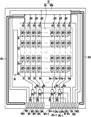
1. A display device, comprising:
a substrate including a display area and a non-display area, the display area including a plurality of pixels electrically connected to a plurality of data lines and to a plurality of scan lines;
a first pad to receive a signal, the first pad including a first test voltage pad and a second test voltage pad separated from each other;
at least one first transistor electrically connected between one of the plurality of data lines of the display area and the first pad;
at least one outline electrically connected between the at least one first transistor and the first pad, the at least one outline being disposed in a non-display area, wherein
the at least one outline comprises a first outline and a second outline separated from each other,
the first outline is electrically connected between a first data line of the plurality of data lines and the first test voltage pad,
the second outline is electrically connected between a third data line of the plurality of data lines and the second test voltage pad, and
the first and second outlines are positioned closest to an edge of the substrate.
|