| CPC H10K 71/00 (2023.02) [H10K 50/865 (2023.02)] | 14 Claims |
|
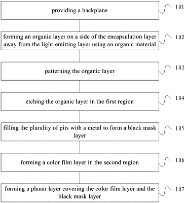
1. A method of manufacturing an OLED display panel, comprising:
providing a backplane, wherein a light-emitting layer is provided on the backplane, and an encapsulation layer is provided on the light-emitting layer;
forming an organic layer on a side of the encapsulation layer away from the light-emitting layer using an organic material;
patterning the organic layer to form, on the encapsulation layer, a first region covered by the organic layer and a second region not covered by the organic layer;
etching the organic layer in the first region to form a plurality of pits on a surface of the organic layer away from the encapsulation layer;
filling the plurality of pits with a metal to form a black mask layer;
forming a color film layer in the second region;
and forming a planar layer covering the color film layer and the black mask layer.
|