| CPC H10K 59/35 (2023.02) [H10K 50/15 (2023.02); H10K 50/16 (2023.02); H10K 50/17 (2023.02); H10K 50/171 (2023.02); H10K 50/19 (2023.02); H10K 59/38 (2023.02); H10K 71/00 (2023.02); H10K 59/122 (2023.02); H10K 59/351 (2023.02); H10K 2102/331 (2023.02)] | 9 Claims |
|
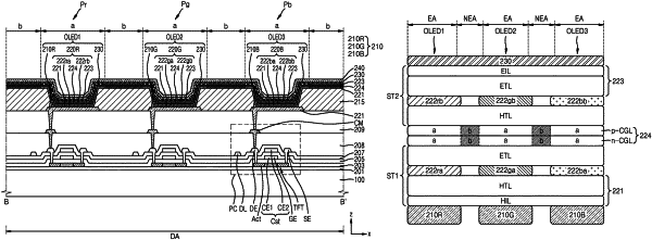
1. A display apparatus comprising:
a first pixel electrode of a first pixel;
a second pixel electrode of a second pixel adjacent to the first pixel, the first and second pixels configured to emit light of different colors from each other;
a first lower emission layer on the first pixel electrode;
a second lower emission layer on the second pixel electrode;
a first upper emission layer on the first lower emission layer;
a second upper emission layer on the second lower emission layer;
a charge generation layer between the first lower emission layer and the first upper emission layer, and between the second lower emission layer and the second upper emission layer; and
a counter electrode extending across the first upper emission layer and the second upper emission layer,
wherein the charge generation layer comprises a first part corresponding to each of the first pixel electrode and the second pixel electrode, and a second part corresponding to an area between the first pixel electrode and the second pixel electrode,
wherein electrical conductivities of the first part and the second part are different from each other, and
wherein the second part of the charge generation layer overlaps with a region where an entirety of the first lower emission layer and an entirety of the second lower emission layer are spaced apart from each other at the area corresponding to the second part of the charge generation layer, and in the region, the second part of the charge generation layer directly contacts a layer extending from underneath the first and second lower emission layers overlapping with the first part of the charge generation layer to the region to overlap with and contact the second part of the charge generation layer.
|