| CPC H10K 59/131 (2023.02) [H10K 50/813 (2023.02); G09G 3/3233 (2013.01); G09G 2300/0426 (2013.01); G09G 2300/0819 (2013.01); G09G 2300/0842 (2013.01); H10K 59/351 (2023.02)] | 20 Claims |
|
1. A display substrate, comprising:
a base substrate;
a pixel circuit layer, on the base substrate;
an anode layer, at a side of the pixel circuit layer away from the base substrate,
wherein the pixel circuit layer comprises a plurality of pixel driving circuits, the anode layer comprises a plurality of anodes, and the plurality of pixel driving circuits are arranged in one-to-one correspondence with the plurality of anodes,
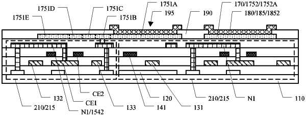
the plurality of anodes comprise a plurality of anode groups arranged in an array along a first direction and a second direction, each of the plurality of anode groups comprises a first anode and a second anode which are oppositely arranged in the second direction, the first anode comprises a first main body portion and a first connection portion, and the first connection portion is electrically connected to a pixel driving circuit corresponding to the first anode,
the first anode further comprises an extension portion and an anode compensation portion, wherein an orthographic projection of the anode compensation portion on the base substrate covers one thin film transistor in the pixel driving circuit connected to the first connection portion,
the first main body portion and the anode compensation portion at least partially overlap in the first direction.
|