| CPC H10K 59/131 (2023.02) [G09G 3/3225 (2013.01); G09G 2300/0408 (2013.01); G09G 2300/0426 (2013.01); G09G 2300/0842 (2013.01); G09G 2320/02 (2013.01)] | 18 Claims |
|
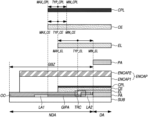
1. A display panel, comprising:
a substrate having a display area and a non-display area;
a gate driving circuit disposed on the substrate in a gate driving circuit area within the non-display area;
a plurality of gate clock lines disposed on the substrate in a first line area positioned outside the gate driving circuit area in the non-display area;
an overcoat layer disposed on the plurality of gate clock lines and the gate driving circuit;
a cathode electrode disposed in the display area and in the non-display area; and
a load deviation compensation pattern disposed in the non-display area and overlapping the plurality of gate clock lines,
wherein the load deviation compensation pattern is a first plate of a capacitor and the plurality of gate clock lines are second plate of the capacitor.
|